


Products
Search

 HDI-SBU technology
1. Introduction
In the development of modern electronic modules, there is a global trend for the level of integration to significantly increase. Apart from the components, of course the printed circuits which accommodate them must follow.
Apart from the general reduction in the widths of structures (track widths and spacings) and the use of blind vias, integration can be further increased by a sequential build up of multilayer boards and the use of buried vias.
The use of buried vias means that holes that go through all layers can be avoided, making more space available on the outer layers to place components.
This information serves as a supplement to the "blind vias" technology information sheet and should help to design a technically optimised and cost-optimised circuit.
You will find extensive, practical recommendations under: Laying out HDI boards for production
2. Explanation of terminology
- HDI (High Density Interconnection): printed circuit with microvias and fine structures
- SBU (Sequential Build Up): sequential build up of multilayer boards with at least 2 pressing processes
- Buried via: this is a through-plated contact (via) which is in the core and is not externally visible
- Blind via: this is a through plated contact (via) which starts on an internal layer & ends on an outer layer
- Microvia: this is a via with diameter < 0.20 mm
An SBU multilayer board is made up of a 2-layer or multilayer core and one or more external, microvia layers.
If buried vias occur in more than 2 layers or in several external microvia layers, then at least 2 pressing procedures will be necessary in the production process.
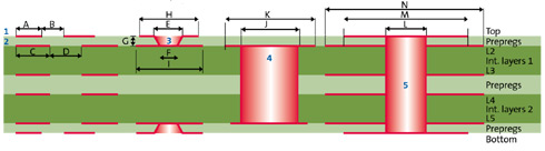
| Symbol | Description | Layout specifications | Comment | |
|---|---|---|---|---|
| 1 | Structure on outer layers | |||
| A | Structure on outer layers | >75 µm | Depends on Cu thickness | |
| B | Track spacing | >75 µm | Depends on Cu thickness | |
| 2 | Structure on inner layers | |||
| C | Track width | >75 µm | Depends on Cu thickness | |
| D | Track spacing | >75 µm | Depends on Cu thickness | |
| 3 | Micro via from top to L2, standard or conic micro drill tool | |||
| E | Hole diameter at entrance | >0.10 mm | If conic, then depends on drilled depth (dielectric thickness) | |
| F | Hole diameter target pad | >0.10 mm | Is defined by the tool | |
| G | Hole depth | Depends on dielectric thickness Top L2 | Note aspect ratio of > 1:1 | |
| H | Micro via entry pad | >E + 200 µm | 100 µm is required all around the hole | |
| I | Micro via pad | >350 µm | F + 125 µm all around the hole diameter on the pad | |
| 4 | Buried via from L2 to L5 | |||
| J | Hole diameter | >0.15 mm | Note aspect ratio of > 1:8 | |
| K | Pad diameter | >L + 200 µm | ||
| 5 | Through hole | |||
| L | Hole diameter | >0.15 mm | Note aspect ratio of > 1:8 | |
| M | Pad diameter Outer layers | >L + 200 µm | 100 µm is required all around the hole | |
| N | Pad diameter Internal layers | >L + 250 µm | 125 µm is required all around the hole |
3. Other options
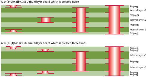
- "b": signifies buried vias i.e. through-plated inner layers or cores
- "( )": layers in brackets are pressed together to form a core in a single step
Important cost factors for SBU boards:
- The number of pressing processes
- The number of drilling programmes (blind & buried vias)
- The number of through-plating processes
4. Steps in the production of a 1+(4)b+1 SBU multilayer board which is pressed twice
- Production of the inner layers
- Press together
- Drill buried vias (all of the way through)
- Through-plate the core of the multilayer board
- Plug holes(optional, if required)
- Production of the core
- Press together
- Drill the blind vias and through holes
- Complete as for a normal multilayer circuit
- For the surface finish, we recommend electroless tin or electroless nickel/gold
5. SBU - Dielectrics
At CONTAG, blind vias are produced by mechanical drilling. This is why consistently good hole quality can be achieved with armoured prepregs as a dielectric for SBU boards. Depending on the layout and the build up of the multilayer board, the prepreg types 106 (about 50 µm thick) and 1080 (about 65 µm thick) have proved to be excellent for standard use. Apart from being good to process, very reliable and with good availability, it is a cheaper material compared to RCC film.
For reliable, high quality manufacturing, the critical steps in the production process are monitored by checking the setup and cutting sections for analysis, as appropriate for the process and job.
- Thickness of the Cu layer in the buried vias (>15 µm specified)
- Precision of the thicknesses and distribution after pressing
- Registration (precision of alignment) of the blind via in the inner layers
- Reliability of connection (hole depth) of the blind vias (15 µm)
- Thickness of the Cu layer in the blind vias (>20 µm specified)

HDI/SBU technology means finest structures and complex multilayer boards. CONTAG has this technology available and of course can also offer these circuits as a rush service.
For further technological questions concerning circuit boards, please contact our team of technologists
(Tel. 030/351 788 155).
Version: D
Your personal contact
+49 30 351 788-333
team contag.de
Quick-Links
 Enquiry, Order
Technologies Blind vias Hole plugging Contact
Enquiry, Order
Technologies Blind vias Hole plugging Contact