


Products
Search
3D-MID
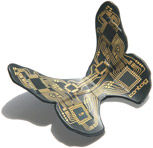
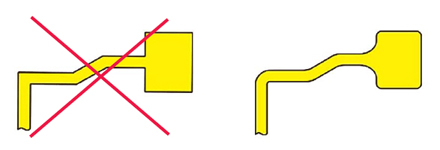
The term 3D-MID (3D moulded interconnect devices) stands for injection-moulded, three-dimensional circuit carriers that have been in use for many years in various fields of application of automotive, mechanical engineering and medical technology up to consumer electronics. In contrast to flexible and rigid-flexible printed circuit boards, which are available in 2D and then finally only in the final stage of the production process. Application can be spatially adapted, MID parts are already produced in 3D manufactured and equipped. This allows a close functional integration of mechanical-constructive and electrical functionality to be possible.
This combination of functionalities opens up completely new possibilities in system development. The portfolio of alternative 3D and 2.5D technologies such as flexible and malleable printed circuit boards is thus supplemented by possibilities that can only be realized in the overall system by MID in a technologically sensible and cost-effective manner. Here 3D-MID offers the intelligent and elegant solution of system development.
CONTAG offers a comprehensive service for 3D-MID projects, from consulting in the design and selection of a suitable material through rapid prototyping to series production and assembly.
2. Material and manufacturing process
a) Rapid-Prototyping
Prototypes and functional models
Rapid prototyping allows 3D-MID prototypes to be produced within a short time and for a manageable budget and functional models. The validation of the design and the functionality gives the security for the success of a project before the investment into the series production. CONTAG relies on 3D printing in combination with laser direct structuring (LDS). Rapid prototyping can also be used for end applications in low quantities.
CONTAG offers stereo lithography 3D printing (SLA) up to a size of 145mm x 145mm x 175mm as a possible method. Compared to other 3D printing processes, the SLA process is characterized by an excellent surface finish and attention to detail. The functional principle is based on the layered curing of a liquid resin using a UV laser. The total number of minimum layer thickness 0.025mm. Thus, high-quality base bodies for 3D-MID prototypes are created from CAD data. The high temp material is a variant that meets the thermal requirements of reflow soldering processes and numerous end applications. In addition, the chemical stability of SLA materials speaks for itself. They are chemically resistant to alkalis, acids, (mineral) oils, fats, hydrocarbons, salt water and hydrogen peroxide.
| Properties | Standard material | High temperature material |
|---|---|---|
| Softening range | 73,1°C | 289°C |
| Breaking point | 65 MPa | 51,1 MPa |
| Stretch | 6,2% | 2% |
Characteristics of stereolithography materials
After 3D printing, the surface of the base body is coated with the special lacquer ProtoPaint, which was developed for the LDS process (see below). Structured laser irradiation activates the paint according to the layout and then metallizes it. Layout structures up to 200μm line/ space can be realized in this way. The glossy black lacquer is characterized by high adhesion and thermo stability and also gives your product a noble character.
b) Small and large series production
For the series production of 3D-MID there are various established processes which CONTAG is proficient in and can provide.
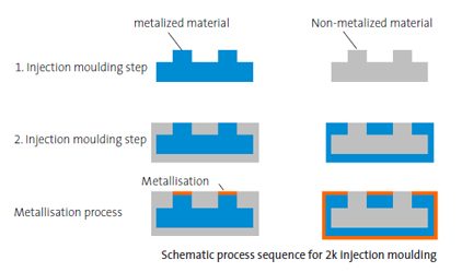
- 2-component injection molding
- 1k injection molding and LDS process
- 1k injection molding based on milled aluminum tools
c) Further materials
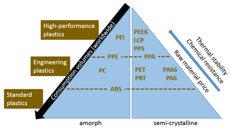
Generally, thermosets are also suitable for 3D-MID applications. In contrast to PCB technology, however, thermosets have so far played a subordinate role for 3D-MID. The thermoplastics, especially the high-performance plastics, meet the requirements in most fields of application. In addition, thermoplastics are easier to process than thermosets due to their thermo formability.
LCP materials (liquid crystal polymer) are widespread representatives of 3D-MID high-performance thermoplastics. These semi-crystalline plastic compounds contain a high degree of fillers and are characterized by excellent thermal and electrical properties as well as very good chemical resistance.
| Characteristics | Value |
|---|---|
| Density | 1,76 g/cm3 |
| Softening range | 277 °C |
| Breaking tension | 1,65 MPa |
| Thermal expansion | x:16 / y:32 ppm/K |
| Moisture absorption | < 0,1 % |
| Thermal conductivity (vertical || parallel) | 0,76 W/m*K || 1,61 W/m*K |
| Dielectric constant εr | 3,8 (1 MHz) |
| Dissipation factor tanδ | approx. 0,03 (1 MHz) |
| Dielectric strength | > 7,5 kV/100 μm |
Physical and electrical properties of an LCP material from RTP
Other general properties:
- Chemically stable to oils, ozone, tar, many solvents and diluted acids
- High UV and weather resistance
- Feasibility of through-plated holes using the additive LDS method
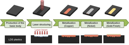
d) Laser direct structuring and metallization
Laser direct structuring (LDS) can be divided into additive and subtractive processes. In the additive LDS process, injection-molded raw materials with a metal-containing additive can be used. Alternatively, such an additive can be applied to the surface of any base body with the Protopaint special lacquer (see above). The metal nuclei are activated for chemical metallization by structured exposure with a laser along the electrical layout.
In addition, the plastic surface is roughened at the exposed areas. Copper can now be chemically deposited at 5-10μm and subsequently refined with the proven ENIG process, for example. For most applications the chemically deposited Cu thickness is completely sufficient, but with appropriate layout planning in advance there is also the possibility of galvanic reinforcement. Depending on the material, the achieved adhesive strength or peel-off force of the chemically deposited copper strips is in the range of 1.4N/mm and thus higher than required by the relevant IPC PCB standard (>1N/mm).
The subtractive LDS process is based on the assumption that the entire surface of the molded part is coated with copper. An etch resist is applied to the surface of this part and structured with the laser. Afterwards the exposed copper surface is etched away and the resist is removed again.
CONTAG offers both the additive and the subtractive LDS method. Depending on design and the desired copper coating is recommended in one or the other variant.
3. Design rules
The electrical layout is a single layer as standard, but also double-sided and through-plated circuits can theoretically be realized. Both the LDS method and the 1k method are used for this purpose. 2k injection moulding process and downstream metallization and assembly processes certain requirements for the design of the basic body and the layout design. These requirements should be considered in the early development phase of your project.
With the LDS method, for example, it is necessary for the laser spot to be positioned as vertically as possible in all areas as this can impinge on the base body along the electrical layout. If the base body is made of an LDS-capable thermoplastic, sharp edges with a large radius should be rounded in order to avoid foreign deposits caused by tool residues. Otherwise, an additional pre-dip process may be necessary, which roughens the surface of the base body and prevents the realizable structure resolution to 200μm line/space.
Any complications caused by thermal stress and solder flow should already be considered during layout design can be counteracted. It is advantageous for stress reduction under temperature stress, avoid sharp-edged changes of direction of the tracks and round the corners of pads on the use of a solder resist can often be dispensed with. However, the transitions of pad and conductive path so that the capillary effect prevents the solder paste from flowing off. The expansion behavior and the maximum size of the components should also correspond to the CTE value of the used thermoplastics in order to achieve a too large offset to the solder contacts to be ruled out.
The recommendations described here are only a selection of the most important design rules for the production of 3D-MID. For further information, please contact the CONTAG team as early as possible. Your technological task will then be checked and the optimal 3D-MID solution will be developed together with you.
| Prototypes / small series | Small and large series | High quantities | |
|---|---|---|---|
| Manufacturing technology | 3D-Druck (SLA) + ProtoPaint + LDS (additiv) | 1k injection moulding + LDS (additive and subtractive) | 2k injection moulding |
| Materials | UV-curing resins | ABS, PA, PBT, PC, LCP, PEEK, etc. | LCP/LCP, LCP/SPS, PBT/ PBT, etc. |
| Min. conductor width/- distance (min. Ø drill hole) | 200μm/200μm | 100μm/100μm | 200μm/200μm (400μm) |
| Advantages | Low initial costs, short delivery time, high flexibility in basic body and layout design | Variety of materials, high flexibility in layout, high structure resolution | Shortened metallization process, favourable for high quantities |
| Disadvantages | Limited mechanical stability and structure resolution | limited flexibility of the basic body | High initial costs, long delivery time, limited flexibility and structure resolution |
Overview of 3D-MID manufacturing technologies at CONTAG
4. Assembly and further processing
If the use of solder resist is necessary, there are two possibilities. On the one hand, before applying solder paste, solder stops can be selectively applied to sensitive areas using a separate processing head of the automatic placement machine. Alternatively, the entire base body is coated with solder resist. In a subsequent laser process, the pad surfaces to be soldered are exposed again.
Common reflow soldering methods can be used for the soldering of pre-assembled components for base bodies made of high-temperature thermoplastics. For thermally sensitive substrates, selective laser soldering or other soldering processes with low-melting solder can be used.
5. Summary and outlook
CONTAG has extensive know-how and offers a convenient complete offer for your 3D-MID project, from consulting in the initial planning phase to rapid prototyping and the production of small and large series. Our drive is the high-quality solution for your technological challenges. CONTAG is a reliable and competent partner for tasks where conventional PCB technologies reach their limits. We draw on an extensive technology pool to develop precisely tailored solutions.
For further technological questions regarding the subject "3D-MID", please contact our CONTAG team (Tel. 030/351 788-300 or team@contag.de).
Version: A
Your personal contact
+49 30 351 788-333
team contag.de
 3D-MID Product info