


Technologies
Search
 Circuits with controlled impedance
1. Introduction
Owing to significantly increasing transmission frequencies, i.e. shorter pulse rise times of electronic components, in high frequency technology, it has become necessary to treat the conductors concerned as a component. Depending upon a number of parameters, HF signals are reflected on circuit boards. This means that the characteristic impedance differs from the output impedance of the transmitting component. The proper transmission of the signal is thus no longer guaranteed.
CONTAG has created the option of checking the required impedance on the customer's circuit board, so as to modify the circuit board, or the tracks and the layer structure if necessary. The impedance is largely determined by the track geometry, the structure of the layers and the dielectric constant (er) of the materials used.
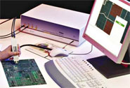
After making the circuit board, the impedances are checked and recorded. The results of the measurements are available on request at any time.
2. Impedances on the circuit board
The standard tolerance used for an impedance is ±10%. Depending upon various PCB characteristics, on request an improved tolerance (down to ±5%) can be offered.
3. Typical models for calculations
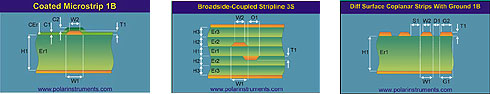
Depending on the complexity of the circuit board, some of the impedances of the circuit board can be checked during the manufacturing process. For this, new models for the corresponding situation (actual state of the circuit board) are separately defined and the results determined.
4. Dielectrics
To make controlled impedance circuit boards, differing materials are used. FR4 is standard here too. However, in applications with very high frequencies (>1 GHz), requirements such as low dielectric loss or a lower er are of increasing importance.
Here, CONTAG can offer a large portfolio of usable materials. Many of these are seen as standard and are regularly used, others are available at short notice. You will find further information in the technology information sheet "Materials".
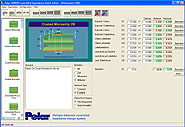
5. Quality control
CONTAG has a CITS900s in their final inspection, the newest test equipment made by POLAR.
6. Design notes
Depositing electroplated copper results in a relatively imprecise and uneven thickness compared to copper foil (for internal layers). For this reason, it is important to think about the manufacture while a circuit board is being developed. In many cases it can make sense to manufacture the layout using tracks with a defined impedance and the associated earth surface on a core, as an internal layer. In this way one of the most important factors, which can falsify the resulting impedance, is eliminated.
The conductors for differential signals should not be too narrow (< 150 µm) and should be routed with sufficiently large separation. To control the impedance of a layout, the circuit board manufacturer has to optimise the layout for their production processes.
For more detailed technological questions on printed circuit boards, please contact our CONTAG-team (+49 30 351 788 - 300 or team@contag.de).
Version: B
Your personal contact
+49 30 351 788-333
team contag.de
Quick-Links
 Enquiry, Order
HDI-SBU technology Multilayer Rigid-flex Contact
Enquiry, Order
HDI-SBU technology Multilayer Rigid-flex Contact