


Technologies
Search
 Carbon Print
1. Introduction
Carbon (also polymer technology) is used for keyboard and LCD contacts and contact pins. The lacquer is based on carbon and can be easily applied to surfaces due to the large content of solids. In this manner, a high surface layer is reached in one application. Due to the high surface rigidity, it is resistant to wear. The lacquer has a resistance of 14 to 20 W/cm² at a dry layer thickness of 25 µm.
2. Application
- Keyboards
- Slide and rotary switches
3. Advantages
- Price advantage in series production (no expensive gold plating)
- More room, since layout guidelines for adjacent different surfaces need not be considered
- Long life due to resistance to corrosion
4. Layout
Since carbon is applied by screen printing, the precision is strongly dependent on the copper thickness. All dimensions in the diagram are in reference to a copper layer thickness of 35 µm. The following layout requirements must be observed:
Carbon coating thickness: 15 30 µm
Carbon print width (min.): 300 µm
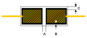
A= Insulation space carbon/carbon ≥ 400 µm
B = Overlap carbon/copper≥ 100 µm
C = Clearance distance copper/soldermask≥ 100 µm
In this manner, with the same values for B + C a defined outline of the carbon lacquer is achieved and run-off is avoided. The carbon lacquer only flows within the soldermask clearance.
For more detailed technological questions on printed circuit boards, please contact our CONTAG-team (+49 30 351 788 - 300 or team@contag.de).
Version: A
Your personal contact
+49 30 351 788-333
team contag.de
Quick-Links
 Enquiry, Order
Products Multilayer HDI-SBU technology Contact
Enquiry, Order
Products Multilayer HDI-SBU technology Contact