


Technologies
Search

 Blind vias
1. Introduction
The integration density of modern electronic modules increases constantly. Apart from the components (µBGA, CSP, FC), the printed circuit board is particularly affected by this. Apart from the general reduction in track widths and spacing, blind vias are a necessary and tried & tested aspect for new design and layout options of printed circuit boards.
When one talks of blind vias today, laser drilling often comes to mind. For series manufacture, this is certainly the only economic, but not the only technically possible solution. Using the most modern CNC (mechanical) drilling machine and special, innovative tools, it is possible, especially when prototyping, to produce mechanically drilled holes of an equal quality and at least equal cost effectiveness.
CONTAG has this technology available and of course can also offer these complex circuits as a rush service. This technology information sheet should help you to design a technically optimised and cost-optimised circuit.
2. Some terms explained
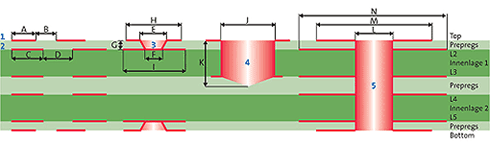
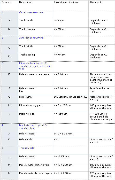
Structure of a 6 layer board with blind vias:
3. Technical details for blind vias
| Outer diameter | Tool | Dielectrics | Aspect ratio |
|---|---|---|---|
| 0.10 mm - 0.40 mm | Standard or conic | Any, standard: FR4 | >=1:1 |
| 0.30 mm - 0.55 mm | Standard (α=130) | Any, standard: FR4 | >=1:1 |
| 0.55 mm - 6.05 mm | Standard (α=130) | Any, standard: FR4 | >=1:1 |
4. Advantages of mechanically drilled blind vias
- Connections over several layers are no problem
- Even larger diameters blind vias are no problem to produce
- Any dielectric materials can be processed
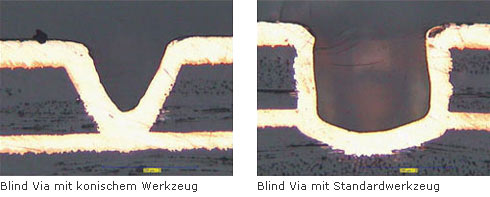
- Maximum connection reliability due to the geometry of the tool
- Maximum precision and reproducibility of the blind via depth by mechanical drilling (±15 µm)
- Very economic when prototyping
5. Quality assurance
Regular checks of the machines and processes as well as set up checks and cutting sections for analysis for particular jobs ensure highest precision in the hole depth, the alignment to the connecting layers as well as the Cu metallisation of the blind vias. We guarantee ≥20 µm Cu thickness in blind vias.
6. Layout guidelines
You will find guidelines on the basic structure of multilayer boards in the "Multilayer" product information sheet. For layout guidelines, especially on the subject of blind vias, the values in the table in section 2 "Some terms explained" will be of use.
7. Summary
For mechanical drilling to depth, vias of any diameter with ideal geometry and maximum connection quality are introduced. When considering the permissible aspect ratios, connections over several layers are just as possible as are microvias with a diameter < 0.20 mm.
Talk to our sales team (+49 30 351 788 - 0 or team
 contag.de). We will look together for a functional, optimised and cost-effective solution for your printed circuit boards.
For more detailed technological questions on printed circuit boards, please contact our CONTAG-team (+49 30 351 788 - 300 or team@contag.de).
Version: C
Your personal contact
+49 30 351 788-333
teamcontag.de
Quick-Links
 Enquiry, Order
Products Multilayer HDI-SBU technology Contact
Enquiry, Order
Products Multilayer HDI-SBU technology Contact